

ASML Unveils Groundbreaking “High NA EUV”
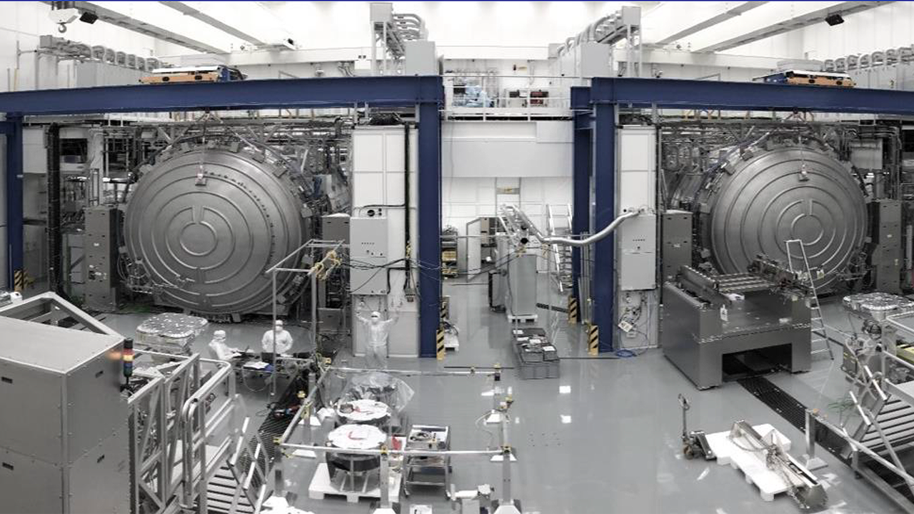
ASML, a leader in chip toolmaking, unveiled its latest innovation: the $350 million “High NA EUV” machine, a crucial component in maintaining its edge in the $125 billion semiconductor market. This device, comparable in size to a double-decker bus, is designed to cater to the needs of top-tier semiconductor manufacturers like Intel and others.
The machine, showcased at ASML’s headquarters in the Netherlands, marks a significant advancement in extreme ultraviolet (EUV) photolithography technology, essential for producing the most advanced chips. ASML anticipates shipping several units this year, although customization and installation remain ongoing tasks.
According to ASML spokesperson Monique Mols, the process involves rigorous engineering and calibration to ensure seamless integration into the manufacturing system, with a steep learning curve for both ASML and its customers.
While the High NA EUV machine represents the next generation of lithography technology, its high cost raises questions about customer adoption. Analysts suggest that while some chipmakers may embrace the new technology early for a competitive edge, the majority may wait until it becomes economically viable, likely around 2030-2031.
ASML’s CEO Peter Wennink believes that the High NA EUV technology offers cost advantages over its predecessors, contrary to some analysts’ predictions. Greet Storms, head of ASML’s High NA product management, predicts an inflection point around 2026-2027 when clients will transition to volume production.
Intel has already received one pilot device and plans to commence production next year, while TSMC and Samsung have expressed intentions to use the tool without specifying timelines. ASML has received between 10 and 20 orders to date, including pilot devices for memory specialists SK Hynix and Micron, with plans to deliver 20 units annually by 2028.
Notably, ASML’s High NA EUV machines will not be available in China due to export restrictions imposed by the United States. However, ASML’s strong order book reassures investors about its performance despite these limitations.
The rapid adoption of the High NA EUV machine could significantly enhance ASML’s sales and margins, solidifying its dominant position in the lithography systems market. This cutting-edge tool enables chipmakers to shrink feature sizes by up to 40%, thereby increasing transistor density nearly threefold.
ASML faces competition from Japanese firms Nikon and Canon in producing lithography machines for older chip generations. However, ASML’s EUV technology, utilizing 13.5 nanometer wavelength light, has established its superiority in the market.
The High NA EUV machine boasts a larger optical system, featuring meticulously polished mirrors made by Carl Zeiss, which collect and focus more light compared to previous models. This innovation, known as high numerical aperture (High NA), contributes to enhanced resolution in chip manufacturing.
Read More Innovation – Tech Foom


